
Note: this post has very little to do with Atredis as company. The only relevance being a part of a consultancy has on this tirade is that its existence has positioned me to be invited back to BlueHat for a second year in a row to talk about whatever seems interesting to me at the time.
This post is a textual version of my talk at Microsoft HQ and honestly more of a manifesto. It intends to define another way to explore your company, another way to look at technological expertise and another path to approach security as a fluid entity, or at the very least, track down Godot.
So, years ago I used to work at the Mitre Corporation. For the uninitiated to the realm, Mitre is a Federally-funded Research and Development Center and can be thought of as a pseudo-government think tank for pseudo-applied research constrained to non-profit status. I entered that organization with a solid career background as a developer specializing in crypto implementations, artificial intelligence and applied game theory. I was quickly tasked, at least in the Mitre sense of the word, with "do something cool and expand yourself". In a decidedly rash "because why the hell not" moment, I picked mobile security and human interactions as my paths of exploration. While I'm sure we will meander into security before the end of this diatribe, I'd oddly enough like to start with problems from the other space.
Specifically at Mitre, I looked at how to foster cross-domain innovation. I basically spent a couple years looking at how new ideas blossom when domain experts from disparate verticals interact and share conceptual structures. I spent weeks modeling building layouts and walking paths trying to ascertain how knowledge spread across the campus. I mapped social networks and interaction structures, I explored forced office mate collaborations and I basically geeked hard on graph theory. I wanted to know how small situational changes could force "Dr. Satellite WaveForm Guru" to stop and share a cup of coffee with "Intern Physicist" and for some reason I always expected robots to fall out of the conversation. Awesome laser wielding autonomous robots that would simply self design more robots and blow things up with lasers while rad 80’s metal blared in the background. I guess I had a thing for robots.
I also wanted data, mounds and mounds of data, to fit into beautiful Gephi graphs that could be analyzed and improved upon. I wanted innovation efficiency. Maybe I thought that the end game was me sitting back in some darkened hivemind control room, watching structured magic happen in realtime, I really don't recall.
I thought that if we could simply control the environment with enough scientific accuracy, we could control that initial "spark" that so many startup books lauded as the beginning of massive scientific breakthroughs. Stated simply, I wanted to play God to a campus of Mensa-level experts. What a surprise it didn't work right? Solving the social graph is a slightly harder problem than raw data collection, who knew?
I did walk away with some insight, that while obvious to most people, had eluded me in the depths of my contrivances. A happenstance chat between two people is almost never really an accident, and it takes a catalyst stronger than a once in an occasional espresso to bond two elements from opposing sides of the periodic table.
In my case, the best catalyst was a bonding agent delivered in the form of an inquisitive procrastinator. An outgoing person who would shirk their own responsibilities and deadlines to randomly walk around and ask people "what are you working on". None of the managers could facilitate these meaningful interactions because they had little insight into what other teams were doing outside of their own silos, and were too damn busy “Getting Things Done”.
A lowly slacker barely hanging onto gainful employment, though, could cross-pollinate like mad. Randomly walking around the building and asking people "whats up, what are you working on?” and then accidentally sharing others problems during small talk. Someone doing that was pure innovation gold. That person was also a huge burden to the immediate bottom line of the company and easily dismissed as a dead end to a small organization. An unrecognized hero that all too often is left with a pink slip and some much needed "forced vacation". [Shawn says: see also Maclolm Gladwell's "The Tipping Point", on influencers and hubs.]
A lowly slacker barely hanging onto gainful employment, though, could cross-pollinate like mad. Randomly walking around the building and asking people "whats up, what are you working on?” and then accidentally sharing others problems during small talk. Someone doing that was pure innovation gold. That person was also a huge burden to the immediate bottom line of the company and easily dismissed as a dead end to a small organization. An unrecognized hero that all too often is left with a pink slip and some much needed "forced vacation". [Shawn says: see also Maclolm Gladwell's "The Tipping Point", on influencers and hubs.]
Let's pause that line of thought for a second and chat about why I sometimes look at Katie Moussouris as the Paul Erdös of Microsoft. If you don't catch it, we will un-pause this conversation when I start talking about degenerates with spray paint.
Paul Erdös was a brilliant mathematician who solved no small amount of insanely difficult problems, but that's not what he is really known for. He crossed into the general public consciousness for his prolific collaboration across fields, he is more than 15-minute Andy Warhol Famous for the Erdös Number. The Kevin Bacon of Academia in a sense.
 |
| Mathematician Paul Erdös. Knuth is his homeboy. |
There are books and websites on this construct, so I'll let the one person reading this unfamiliar with the topic explore at their own pace because I don't care about the number either. I want to point out something less evident.
To some extent, Erdös created a bug bounty in academia. The impetus was vastly different, obviously. I can't speak for Katie or MS, but I don't think either of them wanted to offload problems that would be open and unsolved post personal demise for the simplistic sake of leaving nothing unknown and unexplained. I've never found a definitive source for his original construct, and have always assumed it was an amphetamine-fueled decision process wherein he thought "If I could only be more people, I could solve more problems". A "Fear and Loathing in Las Academia" path to cloning I guess.
Erdös attacked the problem by offering small rewards to those that solved open problems he didn't have time or the mental faculty to tackle himself. He simply outsourced problem solving before there was a term for it. If inquiring minds want to know more, read "Erdös on Graphs" or anything about Fermat's last theorem both will expound upon the program. The problems were (and the open ones still are) immensely hard.
Take a look at the Collatz Conjecture, for example:
Take any natural number n. If n is even, divide it by 2 to get n/2, if n is odd multiply it by 3 and add 1 to obtain 3n+1. Repeat the process indefinitely. The conjecture is that no matter what number you start with, you will always eventually reach 1.
Paul Erdős said about the Collatz conjecture: "Mathematics is not yet ready for such problems." He offered $500 USD for its solution.
Simple, huh? As someone who has wasted a considerable amount of time contemplating this one, I welcome you to join the dark side. It is hard and you have loved ones and friends that need you more, but the outcome would be so fascinating, I really don’t mind you not having nights or weekends
An Erdös check isn't even the type of check you cash, actually. You frame that check and hang it on your office wall when Harvard offers you tenure for being an epic badass. Your prize is writing a page in the book of human knowledge. I might have a slight hero complex here.
Taking a step back though, all Erdös did was to entice random people from random spaces to attack a generic problem. This construct enabled unique points of view to descend upon the same problem space and interact. He seeded the coffee shop with talking points and smart people. He asked a couple of questions and in a sense played God with the outcome.
History and time actually solve the problems, building upon breakthrough after breakthrough. Fermat's Last Theorem itself was solved with a mix of pure innovation and branches of mathematics that are now foundational but were revolutionary or simply non-existent when Fermat trolled the world and much later when Erdos offered up a reward for the joke.
History and time actually solve the problems, building upon breakthrough after breakthrough. Fermat's Last Theorem itself was solved with a mix of pure innovation and branches of mathematics that are now foundational but were revolutionary or simply non-existent when Fermat trolled the world and much later when Erdos offered up a reward for the joke.
 |
| Pierre de Fermat, Legendary Troll |
Treating exploration as foundational knowledge can be seen in most everywhere if you look, but nothing springs to my mind as a better exemplar than graffiti and street art. It is a scene, a lifestyle, legally dubious and in our conversation, a collection of raw transitory data cataloging human interaction. It all starts with an empty wall and one after another people come along and tag it, expand upon it, connect the disparate parts and create a living entity of artistic expression. I guess it would be akin to free form jazz collaboration, but in this instance a city worker washes it away on a scheduled basis and the entire process cycles anew.
Eyesore or museum quality, in this context we don't care about the transitory expression itself. We care about the process and the components that play the game. Every actor has a part in the whole and each person comes into the collaboration with a specific intent and a specific skill set. Every interaction becomes essential to the overall evolution of the art that exists and each artists specialty is a core component of the overall construct.
 |
| London Graffiti |
Let me say the same sentence again with slightly different actors:
Every interaction becomes essential to the overall evolution of the product that ships and each team specialty is a core feature of the overall ecosystem.
If you just woke up from a nice nap with a nightmare about team meetings, I’m sorry and I’ll pause the metaphor break for a bit longer. Consider it a snooze button on the alarm clock of Windows Phone Bluetooth explorations because I want to talk about expertise first.
If I say Kasparov, you probably think about knights and blue mainframes, but let’s drop the mind games and focus on chess for a second. True and utter mastery from our perspective. Not infallible, but an expert by every definition I am aware of. It would be ludicrous to expect anyone in this room to beat a grand master at his or her own game (it could happen, but your ego aside please let me have this statement as fact). Best of 3, 7, 101. As long as we are in the game of chess Kasparov wins. But what if we switch to checkers? Theoretically your odds are better I guess given it is a divergent game, but the outcome is predictable.
What if we extrapolate this out to “all games” though? I’m going to go out on a limb and bet that at least one person reading this could beat Kasparov at Quidditch and probably half of us would win at Texas Hold ‘Em.
 |
| Gary Kasparov, sub-par Quidditch and Poker player |
Expertise mixed with human nature tends to silo itself, specific and targeted perfection normally does not mix with well rounded knowledge. It’s the reason people group themselves by similar interest and it is the reason why my two scientists never made laser wielding robots at Starbucks.
But what if we replace Kasparov with von Neumann, a generally accepted “smart guy” and game theorist at heart. His perfection was not a single game, but the entire construct of a game. Dr. John would not have the skill depth to win against a master, but would understand the implications and theoretical correctness of every move, in every game. Except maybe Quidditch, but probably even that scenario he would see things subtly missed by the lay player. Master in none but “expert” in all? Not really, probably more appropriate to say master in none but meta-understanding in all. He couldn’t beat Kasparov, but he could enumerate where he and Kasparov made mistakes. In a way, he would be qualified to help train and guide a master.
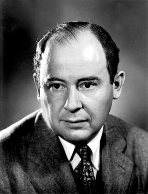 |
| John von Neumann, would build Quidditch state machine |
This was a very long winded way of getting to my point. I want this for you. You are the Kasparov and the Scientist. You have teams that are immensely smart in specific domains and sub-domains and sub-sub-domains, you probably even have a couple slackers helping ideas spread (please don’t fire them, they are your revenue stream in 10 years). What I’m arguing for is a game theory bonding agent, one that can look across silo interactions internal to your products and across all of your competitors.
I want this for you because the real secret is. They are not your competitors. You don’t compete, you innovate and build technology. Other companies do that as well and you share market space with them. Sure, quarterly profit margins make it feel like a race but the longer term reality is that you are responsible for making things better. That is your real place in the game, you construct the future. If you were simply competing, all your advertisements would look like political ads and read “We don’t suck as much as $Product_X”.
From a security perspective, internal teams can tell you exactly what is exposed within the confines of their expertise. If those teams are looking at public security theater they can ensure you are not exposing anything documented with a CVE or any vulnerabilities frozen in YouTube presentations. This should be your base minimal expectation.
One last divergence before my parting thoughts:
Please, please, please don’t ever expect your people to “think outside of the box”. You want experts and that saying is simply “marketechture” and “thinkfluence" bullshit. No one thinks well “outside of the box” because no one is an expert at something they are not an expert at.
All you get with that request is someone fumbling around and maybe getting lucky. Instead, bring an outsider into the process and expect to get another set of eyes on your problem from someone with a completely different view of the world. Someone with a (potentially lesser) expertise in a (potentially) much larger problem space. An outsider brings new context to the thinking process, “thinking outside of the box” kills morale and wastes smart people on silly things.
All you get with that request is someone fumbling around and maybe getting lucky. Instead, bring an outsider into the process and expect to get another set of eyes on your problem from someone with a completely different view of the world. Someone with a (potentially lesser) expertise in a (potentially) much larger problem space. An outsider brings new context to the thinking process, “thinking outside of the box” kills morale and wastes smart people on silly things.
Final tirade aside, if you want to know how your different silos interact within a product, you need someone who understands how that technology works. Generally, you want someone who understands all the technology at a less expert / more meta-theory level. Let that person force both expert teams into understanding consequences outside of their vertical.
If you want to know how your technology implementation compares to other companies selling products, look for someone who has an interest in the overall technology space and don’t try to force them into expertise. In AI I used to search for sub-optimal paths: problems with multiple answers wherein the selected solution was the closest to optimization within the computing constraints. Look for sub-optimal expertise, sometimes you don’t need a PhD for progress. You just need a really excited intern. (Unless it's one of those times you need a PhD).
Do you honestly want to know how your product is going to fare in the post ship-date real world? You need to understand every problem in your technology space, all of the problems in your vendors technology spaces and all of the potential problems from technology that might have conceptually portable attack scenarios.
Trying to secure Bluetooth? I’m sure you have hardened the driver against your hardware, but have you looked at porting all known RFID attacks to your implementation? Do you know what services other vendors expose at the unpaired level of discovery? Have you explored how IoT or RTOS based kernel attacks could be conceptually leveraged against your driver code? If you ever bring in consultants or employees to answer these overall questions and have the realistic intent to use them for anything more than staff augmentation, you should ensure they will do this. You should ensure it excites them and that they want to do it.
Trying to secure Bluetooth? I’m sure you have hardened the driver against your hardware, but have you looked at porting all known RFID attacks to your implementation? Do you know what services other vendors expose at the unpaired level of discovery? Have you explored how IoT or RTOS based kernel attacks could be conceptually leveraged against your driver code? If you ever bring in consultants or employees to answer these overall questions and have the realistic intent to use them for anything more than staff augmentation, you should ensure they will do this. You should ensure it excites them and that they want to do it.
Ok, so you really want to know how to leverage the process used by a good consultant?
Stop trying to make everyone an expert at a thing and start trying to make technology better. Period.
We don’t look at other companies as your competitors, we look at the meta case of “how do we make technology more secure by having fun and breaking things we admire”. You can do the same thing, or you can outsource that to the sub-optimal-experts
We tend to continually learn a technology by looking at all implementations of it. We tend to start with cross domain similarities and extrapolate from there. We look for the general delta between our knowledge base and your product, and we try to minimize that delta.
Thanks,
m0nk
(and I promised I would mention Godot in this diatribe, so… Godot)


